Defect
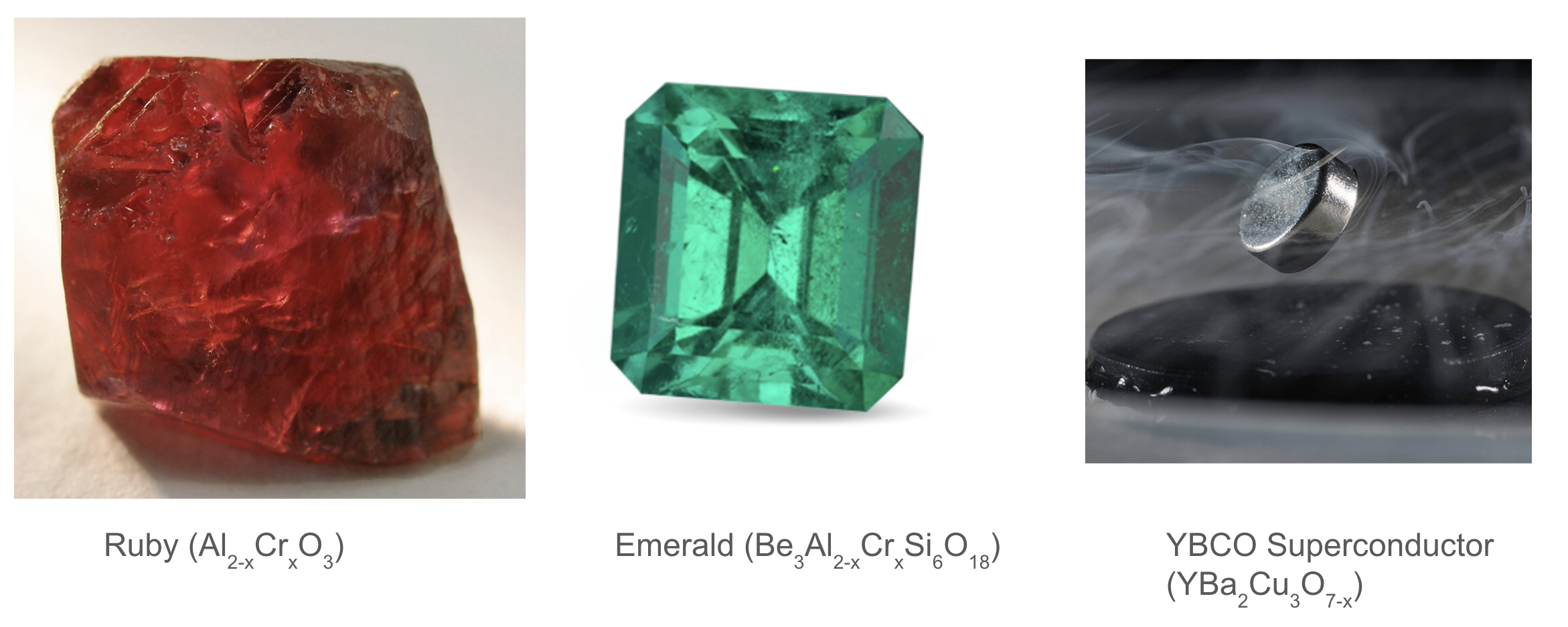
Defects contribute to rubies’ red hue and emeralds’ green coloration, and they are also crucial for enabling superconductivity in YBCO.
In the previous chapter, we discussed the ideal atomic arrangements in crystalline materials. However, in reality, perfect crystals are rare. Most materials contain various types of structural imperfections, such as defects, interfaces, and grain boundaries. These imperfections can significantly influence material properties, including mechanical strength, electrical conductivity, and thermal stability.
Point Defects
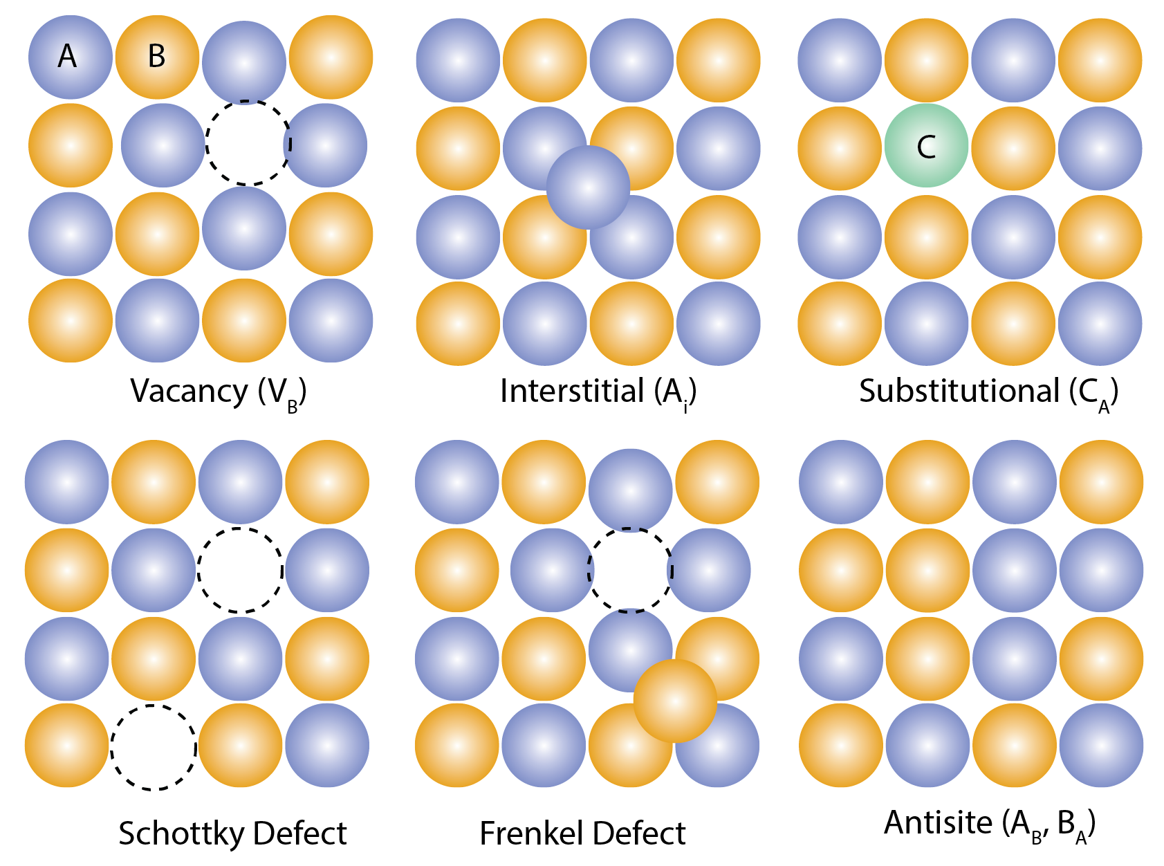
Various types of point defects in crystalline materials.
Point defects represent the simplest deviations from the perfect atomic arrangement in a crystalline material. Imagine a perfectly ordered crystal lattice; a point defect is essentially a localized imperfection involving one or a few atoms. These imperfections can significantly influence a material’s properties, such as its mechanical strength, electrical conductivity, and optical behavior.
We can categorize point defects into several main types: vacancies, interstitials, and substitutional defects.
A vacancy is simply a missing atom from its regular lattice site. Think of it as an empty space where an atom should be. The presence of vacancies disrupts the surrounding crystal structure, leading to local distortions and affecting properties like atomic diffusion rates. A classic example is the Schottky defect, where you have a pair of vacancies, one for a cation and one for an anion, maintaining charge neutrality in ionic compounds.
An interstitial defect occurs when an atom occupies a space between the regular lattice sites. These interstitial atoms squeeze into the structure, causing strain and potentially altering the material’s electronic properties. They can also behave like impurities. A Frenkel defect is a specific type of interstitial defect where an atom has moved from its lattice site to an interstitial site, creating both a vacancy and an interstitial.
Substitutional defects arise when an atom of a different element occupies a regular lattice site. These “foreign” atoms can disrupt the crystal structure and change the material’s properties. Antisites are a specific type of substitutional defect where an atom occupies the “wrong” lattice site (e.g., in a compound AB, an A atom sits on a B site). Antisites are particularly important in complex materials, influencing electronic, optical, and magnetic characteristics.
To describe point defects, we often use Kröger–Vink notation. This is a shorthand notation that tells us the type of defect, its location, and its charge relative to the perfect lattice. For example, represents an oxygen vacancy with a +2 charge relative to the lattice, represents a silicon atom sitting on a carbon site (an antisite), represents an interstitial lithium atom with a +1 charge, and represents a chlorine vacancy with a -1 charge.
It’s important to note that point defects can also carry an electrical charge. These charged defects can significantly impact the electronic properties of the material, influencing conductivity and band structure. Defects that don’t introduce a net charge are called neutral defects.
Point defects play a crucial role in determining various material properties. For instance, they are essential for creating p-type and n-type semiconductors, and they can enhance the catalytic activity of materials like due to the presence of oxygen vacancies ().
Supercell
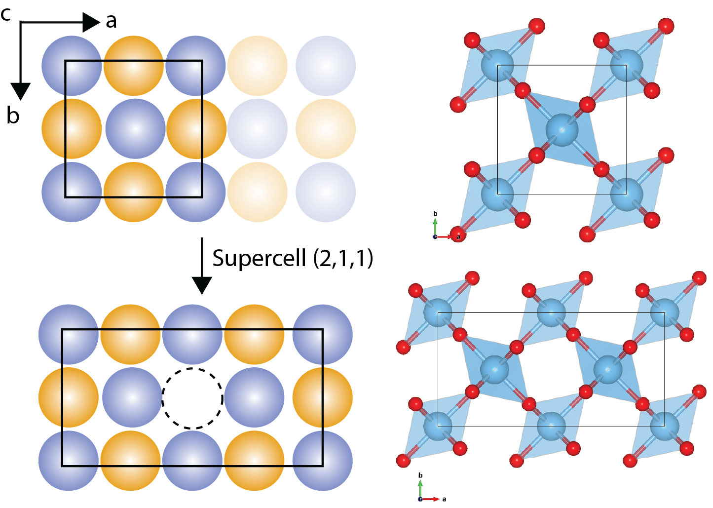
Construction of a supercell with example of
When we want to use computer simulations to study defects, we often employ a technique that relies on “supercells.” Imagine taking the perfect, repeating arrangement of atoms in a crystal and then enlarging it to create a much bigger box – that’s essentially a supercell. We then introduce a defect into this supercell, allowing us to investigate how the defect influences the material’s properties.
Why do we use supercells? Because they allow us to apply periodic boundary conditions, which are a common feature in many simulation methods. By repeating the supercell in all directions, we can mimic an infinite crystal containing a regular array of defects.
However, there’s a catch. The supercell needs to be large enough so that the defect within one supercell doesn’t “feel” the presence of its neighboring defects in the surrounding supercells. If the supercell is too small, the artificial interactions between defects can lead to inaccurate results.
Of course, using a larger supercell comes at a cost. The computational effort required for simulations, especially those based on electronic structure methods, increases rapidly with the size of the supercell. These methods often scale as , where N is the number of atoms, meaning that doubling the supercell size can increase the computational time by a factor of eight!
Another important consideration is that the finite size of the supercell can introduce errors. Because we’re simulating a repeating array of defects rather than a single, isolated defect, we need to apply finite size corrections to minimize these errors. One common method for charged defects is the Freysoldt correction, which accounts for the electrostatic interaction between the charged defect and its periodic images in the simulation. Applying such corrections is crucial for accurately calculating defect formation energies and other important properties.
Other Defects
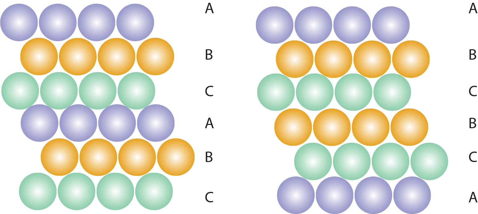
Stacking faults in a crystal structure.
Beyond point defects, crystalline materials may exhibit a variety of additional imperfections, including dislocations, voids, and stacking faults. Dislocations, which are line defects, play a crucial role in plastic deformation and mechanical behavior. Voids represent small empty spaces within the structure, and stacking faults occur when there is an error in the regular sequence of atomic layers.
Modeling these defects poses significant challenges. Their extended nature and complex interactions require advanced simulation techniques and considerable computational resources. Understanding the behavior of these defects is essential for predicting the performance and failure mechanisms of materials.